Printed circuits with thick copper layers
Printed circuits with thick copper layers
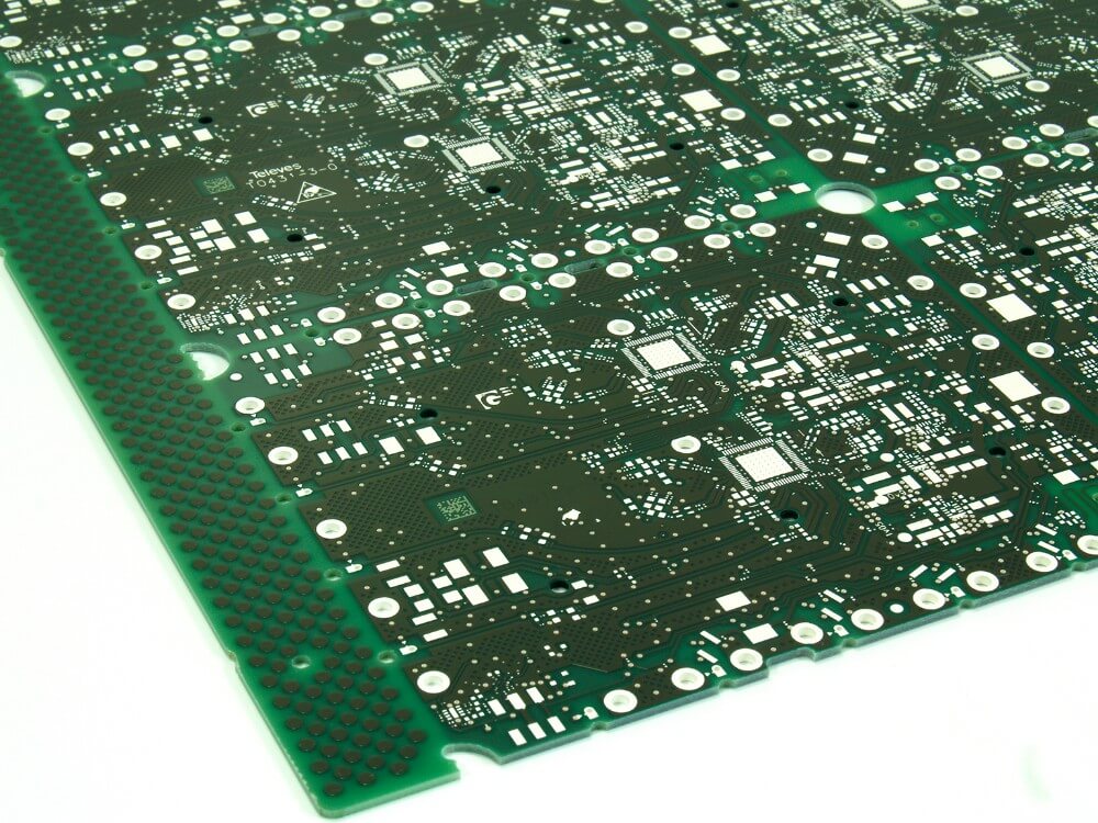
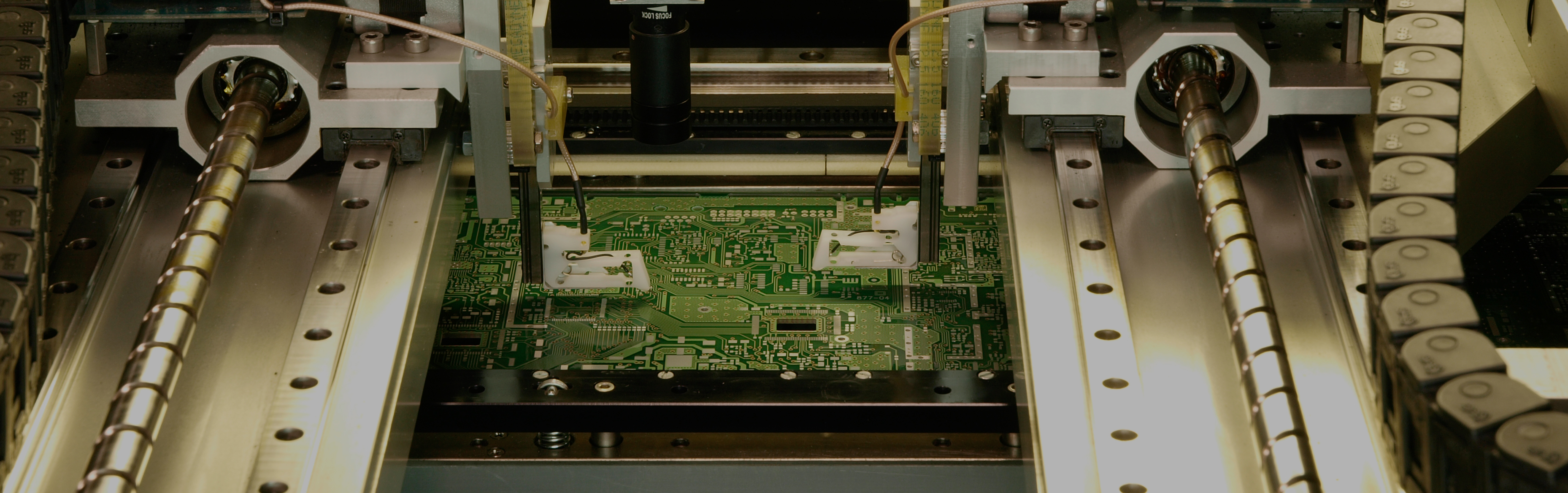
Printed circuits with thick copper layers are high power printed circuits. These PCB have a thick copper surface layer on both internal and external layers, which can range approximately between 70 μm and 400 μm, so as to create well-defined track edges, thinner lines and finer spaces.
This type of circuit has varied applications, which include: solar energy converters, renewable energies, high power rectifiers, overload relays, power and traction converters for railways, electrical line monitors, protection relays, position control systems, nuclear energy applications, line reactors, hydroelectric plants, surge protectors, soldering equipment, weapon control systems, radar systems, etc.
The main advantages of this type of circuit include:
- Increased load current capacity.
- Greater resistance to thermal stress.
- Optimised use of high temperature materials with less likelihood of circuit failure.