


Multi-layer printed circuits
Multi-layer printed circuits
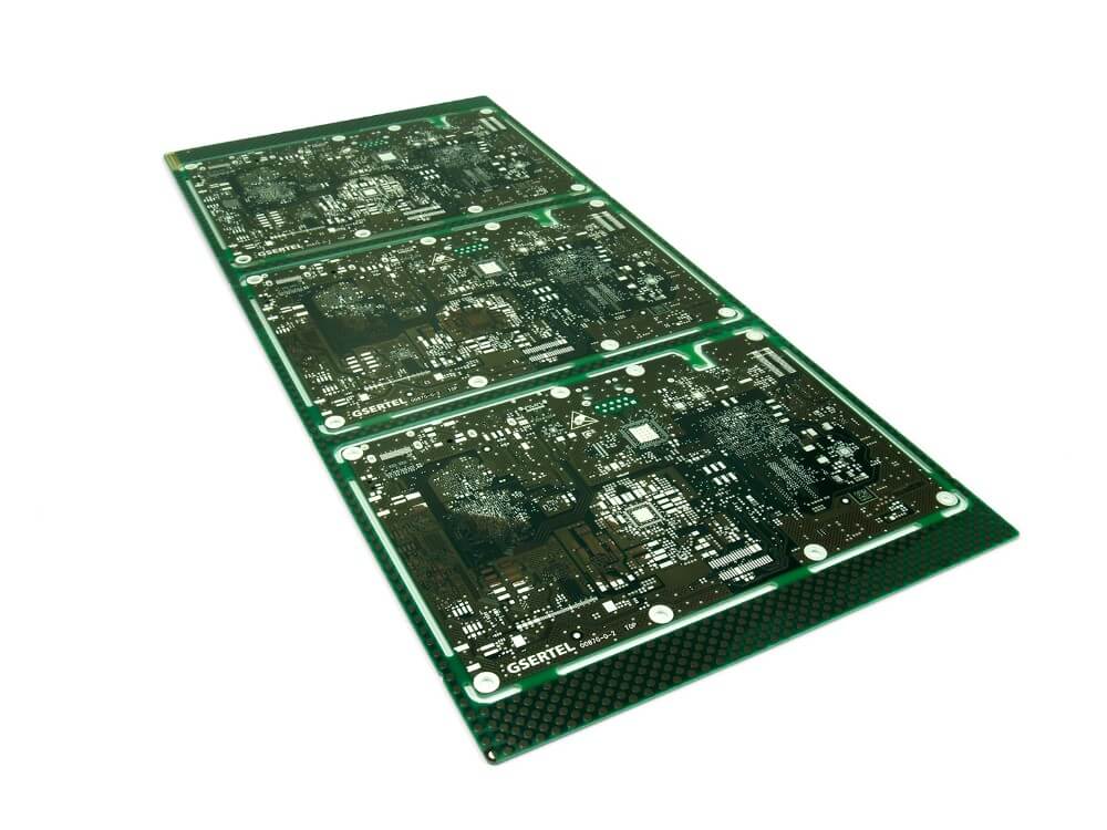
Constant evolution in microelectronics means that multi-layer printed circuits are increasingly more present in our day-to-day. This is due to the modern trend for reducing circuit size while increasing their capacity.
Aware of this market need, at Gallega de Circuits Electrónicos, S.L., we are investing in improving our multi-layer processes to increase production and offer greater quality.

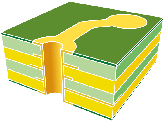
Multi-layer printed circuits are printed circuits with a theoretically unlimited number of isolated conductive layers. These are generally built with double-layer printed circuits on the internal layers, and single-layer on external layers. Prepregs are laminated with no conductive coating so they serve as isolation and heat and pressure are used to bond
loose layers into a multi-layer.
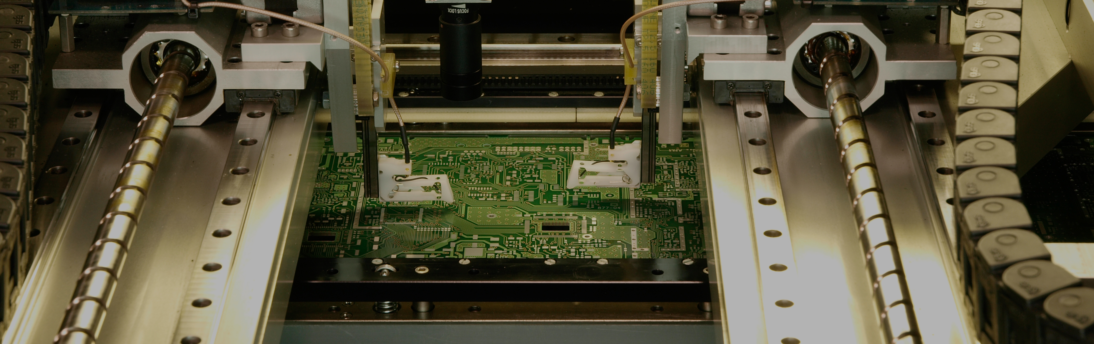
Producing this type of circuit requires a high level of attention to detail as materials must be chosen carefully, as well as construction sequences and the correct placement of sheets, etc.
The most important applications for multi-layer printed circuits are: computers, file servers, data storage, signal transmission, mobile signal boosters, GPS technology, satellite systems, medical X-ray equipment, atomic accelerators, central fire alarm systems, fibre optic receivers,
nuclear detection systems, etc.
The main advantages over single-layer and double-layer circuits include:
- Greater assembly density.
- Smaller size (considerable space savings).
- Greater flexibility.
- Easier to incorporate controlled impedance characteristics.
| CHARACTERISTICS | IMAGE | CATEGORY 3 | CATEGORY 4 | CATEGORY 5 | CATEGORY 6 | CATEGORY 7 |
|---|---|---|---|---|---|---|
| Minimum metallic hole. | 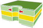 |
0.7 | 0.6 | 0.4 | 0.2 | 0.15 |
| Minimum NON metallic hole. | 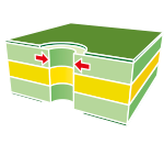 |
0.8 | 0.7 | 0.5 | 0.3 | 0.25 |
| Ratio between circuit thickness and hole. | 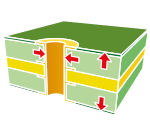 |
5 | 5 | 6 | 8 | 13 (Maximum thickness) |
| Minimum track width on external layers. |  |
0.30 | 0.20 | 0.15 | 0.125 | 0.100 |
| Minimum space between tracks on external layers. | 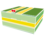 |
0.25 | 0.20 | 0.15 | 0.125 | 0.100 |
| Minimum track width on internal layers. | 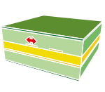 |
0.25 | 0.20 | 0.150 | 0.125 | 0.100 |
| Minimum space between tracks on internal layers. | 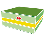 |
0.25 | 0.20 | 0.150 | 0.125 | 0.100 |
| Minimum distance between crown and hole on external layers. | 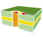 |
0.250 | 0.200 | 0.150 | 0.125 | 0.100 |
| Minimum crown on internal signal layers. | 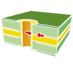 |
0.25 | 0.23 | 0.20 | 0.160 | 0.130 |
| Minimum distance between metallic hole and tracks. | |
0.425 | 0.400 | 0.325 | 0.25 | 0.200 |
| Minimum diameter for blind vias. | 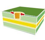 |
— | — | — | 0.40 | 0.120 |
| Minimum crown for blind vias. | 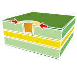 |
— | — | — | 0.350 | 0.250 |
| Minimum internal crown for blind vias. | 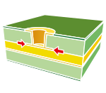 |
— | — | — | 0.350 | 0.250 |
| Minimum insulation thickness on blind vias. | 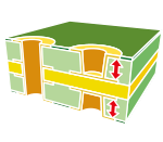 |
— | — | — | 0.115 | 0.080 |
| Maximum error in slot position. | 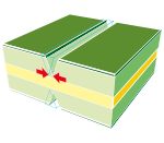 |
0.125 | 0.125 | 0.125 | 0.125 | 0.100 |
| Tolerances for slot nerve. | 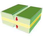 |
0.200 | 0.200 | 0.200 | 0.200 | 0.150 |
| Contour dimensions |  |
0.150 | 0.150 | 0.150 | 0.150 | 0.100 |
| Minimum tolerances between conductors for slotting. | 1.00 | 1.00 | 1.00 | 1.00 | 0.800 | |
| End thickness. | 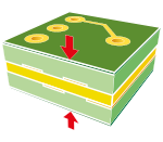 |
±0,100 | ±0,100 | ±0,100 | ±0,100 | ±0.05 |
| Thickness between layers. | 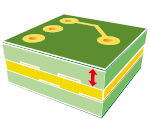 |
±0,060 | ±0,060 | ±0,060 | ±0,060 | ±0,060 |
| Metallisation thickness in through hole. | 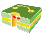 |
>0.020 | >0.020 | >0.020 | >0.020 | >0.025 |
| Metallisation thickness in blind_buried holes. |  |
>0.025 | >0.025 | >0.025 | >0.025 | >0.025 |
| Metallisation thickness in blind via. | 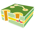 |
>0.025 | >0.025 | >0.025 | >0.025 | >0.025 |
| Minimum wall between NON metallic holes. | 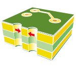 |
0.250 | 0.250 | 0.250 | 0.250 | 0.200 |
| Minimum crown for NON metallic hole. |  |
0.250 | 0.250 | 0.250 | 0.200 | 0.200 |
| Minimum distance between conductor and NON metallic hole. |  |
0.200 | 0.200 | 0.200 | 0.200 | 0.125 |
| Minimum distance between conductor and contour. |  |
0.200 | 0.200 | 0.200 | 0.200 | 0.125 |
| Maximum deviation between contour and hole | 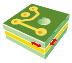 |
0.200 | 0.200 | 0.200 | 0.125 | 0.075 |
| Maximum deviation between pad and hole (EXTERNAL faces). |  |
0.100 | 0.100 | 0.100 | 0.100 | 0.075 |
| Maximum deviation between pad and hole (INTERNAL faces). |  |
0.125 | 0.125 | 0.125 | 0.125 | 0.125 |
| Maximum deviation between copper and photosensitive mask. | 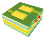 |
0.150 | 0.150 | 0.150 | 0.150 | 0.075 |
| Minimum photosensitive ink stroke. | 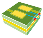 |
0.100 | 0.100 | 0.100 | 0.100 | 0.075 |
| Minimum allowance for photosensitive ink. | 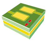 |
0.075 | 0.075 | 0.075 | 0.075 | 0.050 |
| Minimum width for legend trace. | 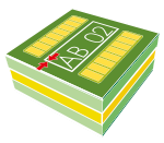 |
0.150 | 0.150 | 0.150 | 0.150 | 0.125 |
| Minimum allowance for graphite ink. |  |
0.200 | 0.200 | 0.200 | 0.200 | 0.150 |
| Minimum space between graphite ink. |  |
0.450 | 0.450 | 0.450 | 0.450 | 0.400 |
| Minimum allowance between graphite and conductor. |  |
0.350 | 0.350 | 0.350 | 0.350 | 0.350 |
| Minimum allowance for peelable ink. |  |
0.900 | 0.900 | 0.900 | 0.900 | 0.700 |
| Minimum distance between pad and peelable ink. |  |
0.900 | 0.900 | 0.900 | 0.900 | 0.700 |
| Minimum distance between contour and peelable ink. | 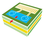 |
0.900 | 0.900 | 0.900 | 0.900 | 0.700 |
| Maximum diameter for hole covered with peelable ink. |  |
1.90 | 1.90 | 1.90 | 1.90 | 2.10 |