


Single-layer printed circuits
Single-layer printed circuits
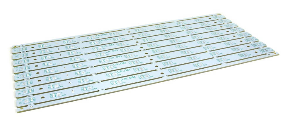
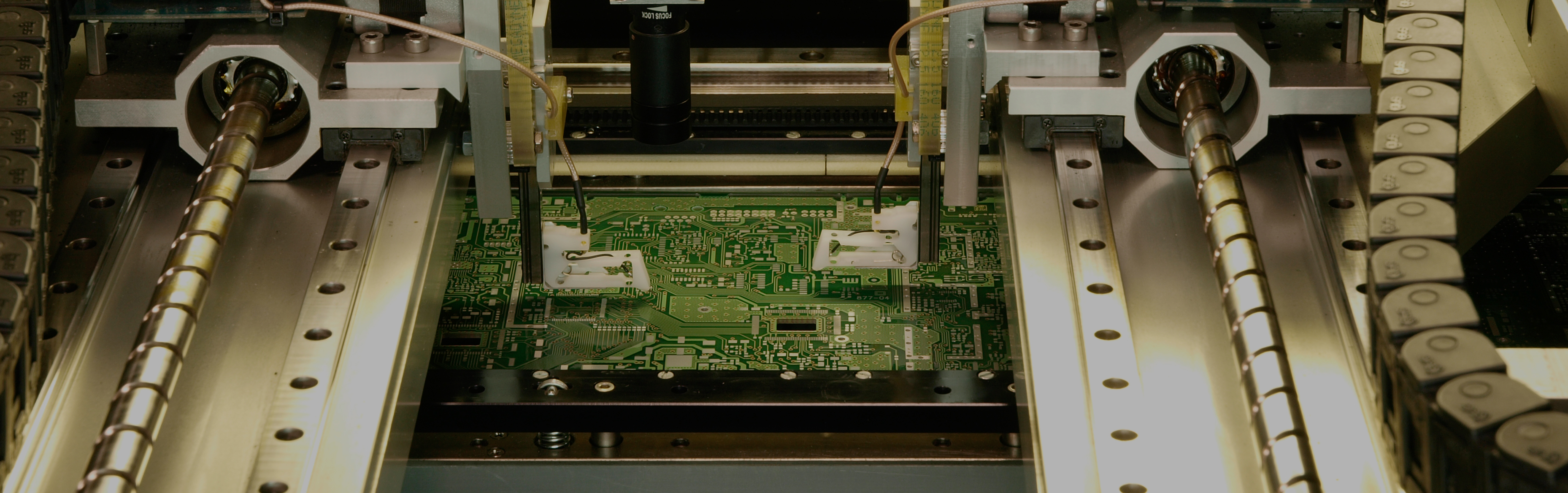
Single-layer printed circuits have been around since the ‘50s and still dominate the world market in volume of parts as they are simple and quick to manufacture and design.

They contain just one layer of thermally conductive but electrically isolating dielectric material covered with a layer of copper, and they are best suited for low density designs. However, although they are relatively simple, they are used in highly complex devices such as: power sources, relays (automotive and industrial), LED lighting, radio and sound equipment, packaging equipment, surveillance, calculators, printers, coffee machines, vending machines, etc.
And Gallega de Circuitos Electrónicos, S.L. offers this type of circuit in all kinds of materials (FR4, High Tg, Halogen Free, Aluminium, Ceramic, High Frequency, etc.), with copper thickness ranging from 9 μm to 400 μm, and with all available finishes.
The main advantages of this type of circuit include:
- Ideal for simple, low density designs.
- Lower costs, especially for high-volume orders.
- Less likelihood of manufacturing problems.
- Popular, common and easy to understand by most PCB manufacturers.
| CHARACTERISTICS | IMAGE | CATEGORY 1 | CATEGORY 2 |
|---|---|---|---|
| Minimum NON metallic hole |  |
0.8 | 0.5 |
| Minimum track width on external layers. |  |
250 | 150 |
| Minimum space between tracks on external layers. |  |
250 | 150 |
| Minimum distance between crown and hole on external layers. |  |
0.300 | 0.250 |
| Maximum error in slot position. |  |
0.150 | 0.125 |
| Tolerances for slot nerve |  |
+-0.250 | +-0.200 |
| Contour dimensions |  |
0.200 | 0.150 |
| Minimum tolerances between conductors for slotting. | 1.00 | 0.800 | |
| End thickness. |  |
+-0.100 | +-0.100 |
| Minimum wall between NON metallic holes. | 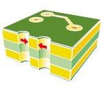 |
0.300 | 0.250 |
| Minimum crown for NON metallic hole. | 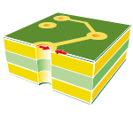 |
0.350 | 0.250 |
| Minimum distance between conductor and NON metallic hole. |  |
0.250 | 0.200 |
| Minimum distance between conductor and contour. | 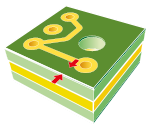 |
0.250 | 0.200 |
| Maximum deviation between contour and hole. | 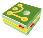 |
0.250 | 0.200 |
| Maximum deviation between copper and photosensitive mask. | 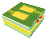 |
0.200 | 0.150 |
| Minimum photosensitive ink stroke. | 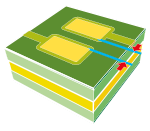 |
0.200 | 0.100 |
| Minimum allowance for photosensitive ink. | 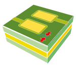 |
0.100 | 0.075 |
| Minimum width for legend trace. | 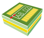 |
0.150 | 0.125 |
| Minimum allowance for graphite ink. |  |
0.400 | 0.200 |
| Minimum space between graphite ink. |  |
0.450 | 0.450 |
| Minimum allowance between graphite and conductor. | 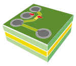 |
0.450 | 0.450 |
| Minimum allowance for peelable ink. |  |
1.00 | 0.900 |
| Minimum distance between pad and peelable ink. |  |
1.00 | 0.900 |
| Minimum distance between contour and peelable ink. | 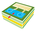 |
1.00 | 0.900 |
| Maximum diameter for hole covered with peelable ink. | 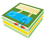 |
1.900 | 1.900 |