


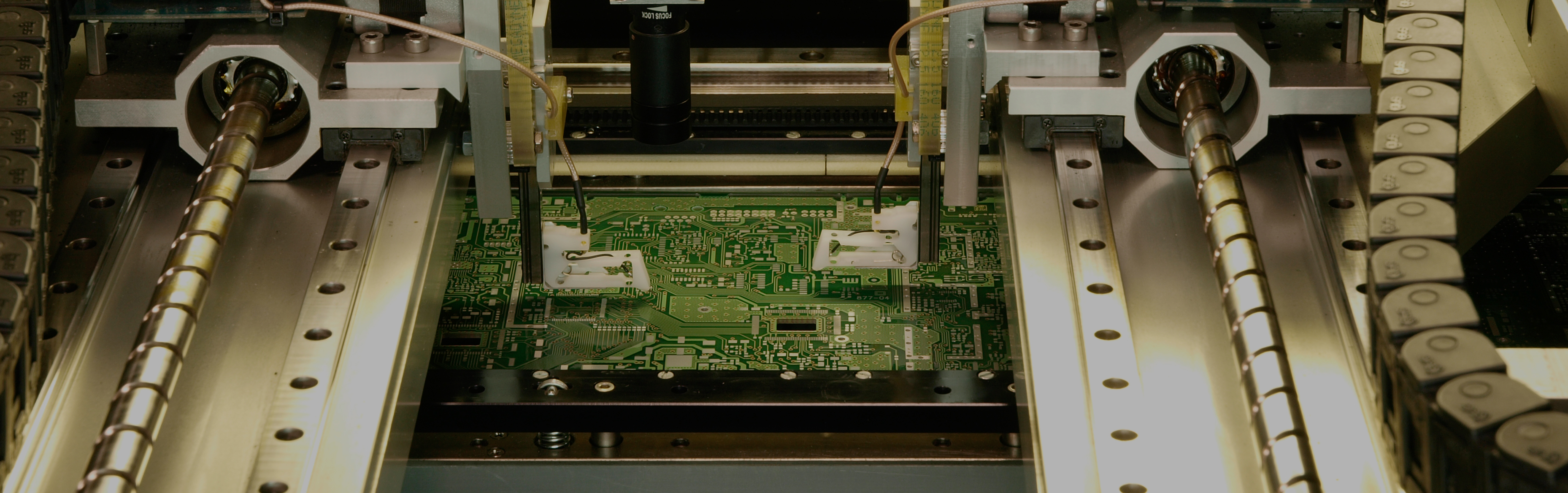
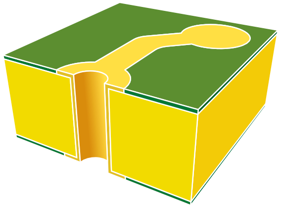
Double-layer printed circuits
Double-layer printed circuits
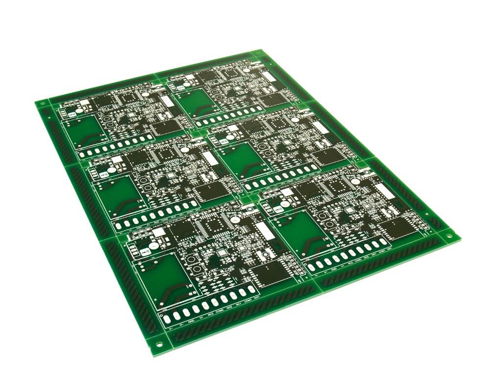
Nowadays, double-layer printed circuit technology is perhaps the most popular type of PCB in the industry and they support advanced technology applications.

The main applications for this type of printed circuit include: industrial controllers, power sources, converters, control relays, instruments, energy conversion systems, LED lighting, hard drives, printers, telephone systems, energy control systems, line reactors, amplifiers, traffic systems, vending machines, etc.
The main advantages of this type of circuit include:
- Greater flexibility for designers.
- Higher circuit density.
- Relatively low costs.
- Intermediate circuit complexity.
- Reduced circuit size (which reduces costs).
| CHARACTERISTICS | IMAGE | CATEGORY 3 | CATEGORY 4 | CATEGORY 5 | CATEGORY 6 | CATEGORY 7 |
|---|---|---|---|---|---|---|
| Minimum metallic hole. |  |
0.7 | 0.5 | 0.4 | 0.3 | 0.2 |
| Minimum NON metallic hole. | |
0.8 | 0.6 | 0.5 | 0.4 | 0.3 |
| Ratio between circuit thickness and hole. | 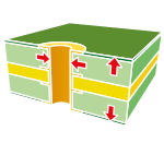 |
3 | 5 | 10 | 15 | 15 |
| Minimum track width on external layers. | 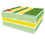 |
0.250 | 0.200 | 0.150 | 0.125 | 0.100 |
| Minimum space between tracks on external layers. | 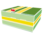 |
0.250 | 0.200 | 0.150 | 0.125 | 0.100 |
| Minimum distance between crown and hole on external layers. | 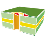 |
0.250 | 0.200 | 0.150 | 0.125 | 0.100 |
| Maximum error in slot position. |  |
0.125 | 0.125 | 0.125 | 0.125 | 0.100 |
| Tolerances for slot nerve. |  |
±0.2 | ±0.2 | ±0.2 | ±0.2 | ±0,150 |
| Contour dimensions |  |
±0,150 | ±0,150 | ±0,150 | ±0,150 | ±0,100 |
| Minimum tolerances between conductors for slotting. | 1.0 | 1.0 | 1.0 | 1.0 | 0.8 | |
| End thickness. |  |
±0,100 | ±0,100 | ±0,100 | ±0,100 | ±0.75 |
| Metallisation thickness in through hole. |  |
>0.020 | >0.020 | >0.020 | >0.020 | >0.025 |
| Minimum wall between NON metallic holes. | 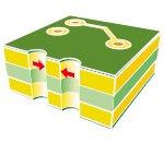 |
0.250 | 0.250 | 0.250 | 0.250 | 0.200 |
| Minimum crown for NON metallic hole. | 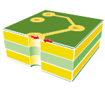 |
0.300 | 0.250 | 0.250 | 0.250 | 0.200 |
| Minimum distance between conductor and NON metallic hole. |  |
0.200 | 0.200 | 0.200 | 0.200 | 0.150 |
| Minimum distance between conductor and contour. | 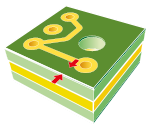 |
0.200 | 0.200 | 0.200 | 0.200 | 0.125 |
| Maximum deviation between contour and hole. | 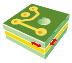 |
0.200 | 0.200 | 0.200 | 0.200 | 0.125 |
| Maximum deviation between pad and hole (EXTERNAL faces). | 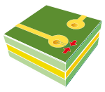 |
0.100 | 0.100 | 0.100 | 0.100 | 0.075 |
| Maximum deviation between copper and photosensitive mask. | 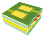 |
0.150 | 0.150 | 0.150 | 0.150 | 0.075 |
| Minimum photosensitive ink stroke. | 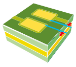 |
0.100 | 0.100 | 0.100 | 0.100 | 0.075 |
| Minimum allowance for photosensitive ink. | 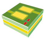 |
0.075 | 0.075 | 0.075 | 0.075 | 0.050 |
| Minimum width for legend trace. | 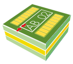 |
0.150 | 0.150 | 0.150 | 0.150 | 0.125 |
| Minimum allowance for graphite ink. |  |
0.200 | 0.200 | 0.200 | 0.200 | 0.150 |
| Minimum space between graphite ink. |  |
0.450 | 0.450 | 0.450 | 0.450 | 0.350 |
| Minimum allowance between graphite and conductor. | 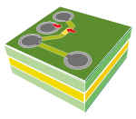 |
0.350 | 0.350 | 0.350 | 0.350 | 0.300 |
| Minimum allowance for peelable ink. | 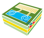 |
0.900 | 0.900 | 0.900 | 0.900 | 0.700 |
| Minimum distance between pad and peelable ink. |  |
0.900 | 0.900 | 0.900 | 0.900 | 0.700 |
| Minimum distance between contour and peelable ink. |  |
0.900 | 0.900 | 0.900 | 0.900 | 0.700 |
| Maximum diameter for hole covered with peelable ink. | 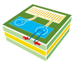 |
1.90 | 1.90 | 1.90 | 1.90 | 2.10 |